In order to better support the MegaSquirt-II processor, the MegaSquirt® printed circuit board has been updated. The new MegaSquirt® Version 3 (V3) board incorporates a host of new features and improvements over the previous V1.01 and V2.2 board versions. It now features:
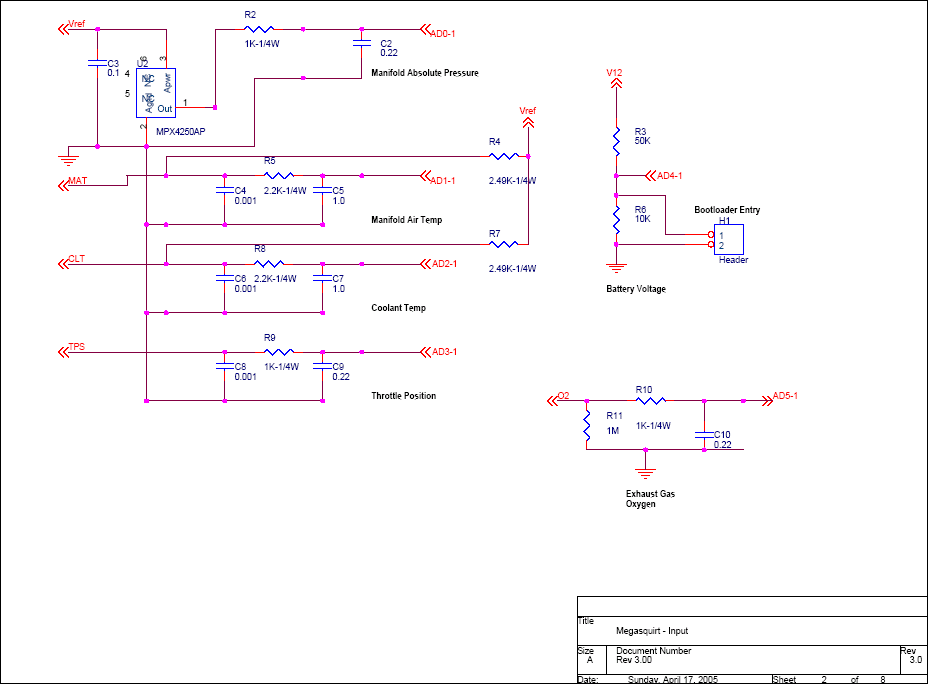
As well, the remaining two ADCs with circuits have been brought out, mirroring the MAT/CLT sensors. Having the ADC come out with the low-pass filter resistor/cap that then terminates to a jumper hole would be helpful. Users can then run a jumper to wherever they want.
For the new MegaSquirt® V3 main board, the case will be the same as used for the other MegaSquirt® boards (LMB 6x4 case or equivalent), however the end-plates are different as the DB connectors have moved.
However there are changes to both the front and rear panel. The driving force behind this was the use of an integrated heat sink "bus bar" setup. The heat sink is mode out of a easy to obtain 3/4" x 1/8" flat aluminum stock cut 6 inches long. This bus bar mounts across the top side of the PCB and all of the TO-220 power devices mount on this (there are 10 of 'em - the regulator, two drive FETs, two power Zener circuits, two flyback dampers, two TO-220-packaged power resistors-the 0.050-ohm for overcurrent detection, and the IGBT). The TO-220 devices mount to a simple 3/4" x 1/8" flat aluminum strip, 6 inches long, laid on the PCB top with the TO-220 packages bent over and screwed down thru the angle and PCB (much like the flyback board right now). This provides greatly increased heat sink capability, and even with a 3-injector (1.2 ohm) per bank load at 3K RPM the overall sink stays cool.
Note that the entire flyback circuit is on the board, as is a 12 amp overcurrent foldback circuit (the two large black rectangles on the heat sink w/ two leads are power resistors). The driver stage should be bulletproof to overheating and overcurrent.
The new board is a 4-layer board, meaning that there are separate power and ground planes sandwiched inside. The power and ground plane really helps in noise immunity and component routing. Also not visible is the fact that all of the high power components (injector, ignition) have a separate ground return path and traces back to the connector by itself without connecting to the digital/analog power planes. The injector driver output traces themselves are on the inner layers as copper pour areas back to the connector.
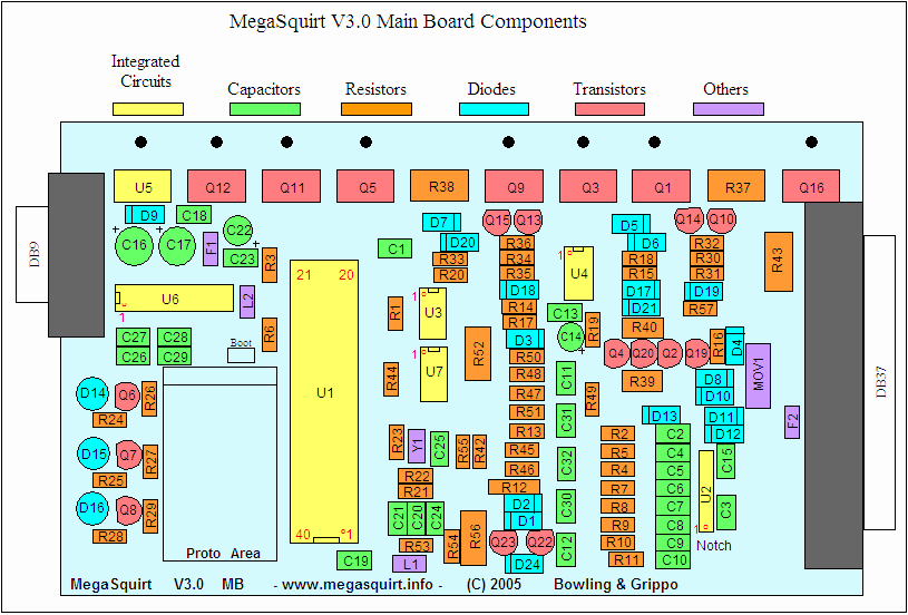
Note that there are many more components on the board, which has led to putting the silk screen labeling under many of the components. Not much that can be done due to the density of the board (less real-estate due to the heat sink and proto area and more components) - we will provide a component silkscreen map that people can follow. Same goes with part numbering, components on this board have different part designations compared to the other boards. There are so many new components on this board that it was hard to keep everything the same, so it was chosen to renumber everything, but this time the numbers are consecutive. This makes it a little harder to compare circuit mods with V2.2 and older, but this board has many of the mods and the prototype area will be the major area of focus for new circuitry which will need new documentation.
The V3 main board is now available in either 96HC908 (MegaSquirt/MSnS-E) or MegaSquirt-II partial kit form from Bowling and Grippo at:
Order MSPKIT for the 98HC908 processor (MegaSquirt or MSnS-E code) or MS2PKIT for MegaSquirt-II daughter cards. MegaSquirt® distributors may sell complete V3 kits, check the 'Products and Distributors' forum at www.msefi.com
The Digi-Key BOM automated ordering page for the V3 main board is here:
The assembly guide for the V3 main board is here:
The parts orientation is here:
There is a copper area along the top - this is where the heat sink runs across the board. Also, this copper area is the ground plane for all of the power driver circuits - notice that it hooks over to the right and down to the connector pins. All power ground currents flow on this plane layer. Not shown is the ground plane for the processor+components, this is on an inner layer which also joins the connector (but this is on a different layer). So the ground plane for the power devices and the ground plane for the processor meet up right through the connector pins. None of the high-currents for the injectors or IGBT flow on the processor ground plane. Also, the XG2 ground pin for the optoisolator is routed to the power driver ground plane and not the processor ground plane.
Also not shown is the that below the ground plane for the power devices (below the square tube area) there are three more routing layers - each layer is used to route one of the three power circuits (two injector drivers and the IGBT) directly to the connector via wide traces.
The MAP sensor has also been moved to the bottom and should be close enough that the barb protrudes slightly beyond the rear cover, enough to easily slip on a vacuum hose.
The components have been re-numbered. The change in reference designators for the V3 board was not taken lightly. But with all of the change of the circuitry and the inclusion of the flyback board it was very hard to keep the same numbering. Plus, the original V1.01 and V2.2 main boards had gaps, etc. in the sequence of numbers. So, everything is renumbered.
This is really not just the same old MegaSquirt® when it comes to build or support. The main difference is all of the build options that people can do - here are a few listed:
People will have to get used to identifying which board they have - easy to do since the v3 main board has the prototype area and is an easy key to the board they have. This is the result of fulfilling the general request for the added options.
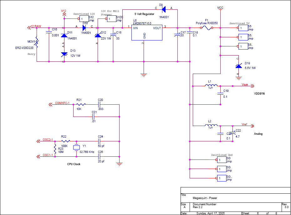
The MegaSquirt-II PCB receives electrical current along from the vehicle's battery. If the voltage from the charging system surges or spikes (rises above the accepted level) the Metal Oxide Varistor (MOV) diverts just enough current into the outlet's grounding wire to keep the voltage supply to the components at the acceptable level.
A MOV forms a connection between the hot power line and the grounding line. A MOV has three parts: a piece of metal oxide material in the middle, joined to the power and grounding line by two semiconductors.
These semiconductors have a variable resistance that is dependent on voltage. When voltage is below a certain level, the electrons in the semiconductors flow in such a way as to create a very high resistance. When the voltage exceeds that level, the electrons behave differently, creating a much lower resistance to ground. When the voltage is correct, an MOV does nothing. When voltage is too high, an MOV can conduct 'excess' current to ground in order to eliminate the extra voltage.
Because the extra current is diverted into the MOV and to ground, the voltage in the PCB power supply line returns to a normal level, so the MOV's 'by-pass' resistance shoots up again. In this way, the MOV only diverts the surge current, while allowing the standard current to continue powering the components on the PCB.
MegaSquirt v3.0 PCB Schematics
Please note that a few component values may have been tweaked - especially in the VR input circuit, but possibly others as well. Follow the BOM values for the current component specifications and use these over the values listed on the following schematics.
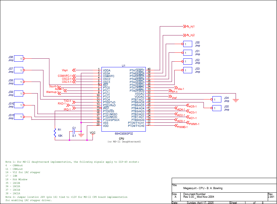
Note 1: For MS-II daughter card implementation, the following signals apply to DIP-40 socket:
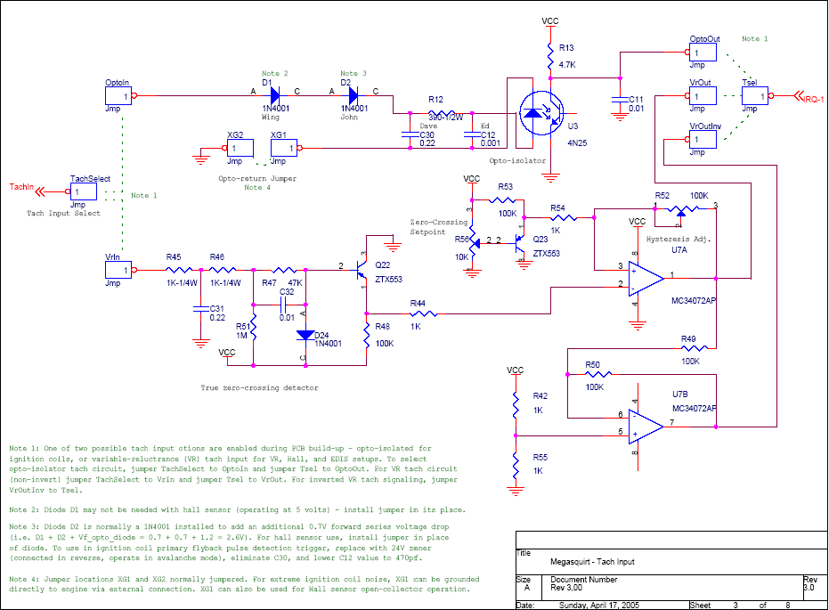
Note 1: One of two possible tach input options are enabled during PCB build-up:
To select opto-isolator tach circuit, jumper TachSelect to OptoIn and jumper Tsel to OptoOut. For VR tach circuit (non-invert) jumper TachSelect to VrIn and jumper Tsel to VrOut. For inverted VR tach signaling, jumper VrOutInv to Tsel.
Note 2: Diode D1 may not be needed with Hall sensor (operating at 5 volts) - install jumper in its place.
Note 3: Diode D2 is normally a 1N4001 installed to add an additional 0.7V forward series voltage drop (i.e. D1 + D2 + Vf_opto_diode = 0.7 + 0.7 + 1.2 = 2.6V). For Hall sensor use, install jumper in place of diode. To use in ignition coil primary flyback pulse detection trigger, replace with 24V Zener (connected in reverse, operate in avalanche mode), eliminate C30, and lower C12 value to 470 pF.
Note 4: Jumper locations XG1 and XG2 normally jumpered. For extreme ignition coil noise, XG1 can be grounded directly to engine via external connection. XG1 can also be used for Hall sensor open-collector operation.
Please note that a few component values may have been tweaked - especially in the VR input circuit, but possibly others as well. Follow the BOM values for the current component specifications and use these over the values listed on these schematics.
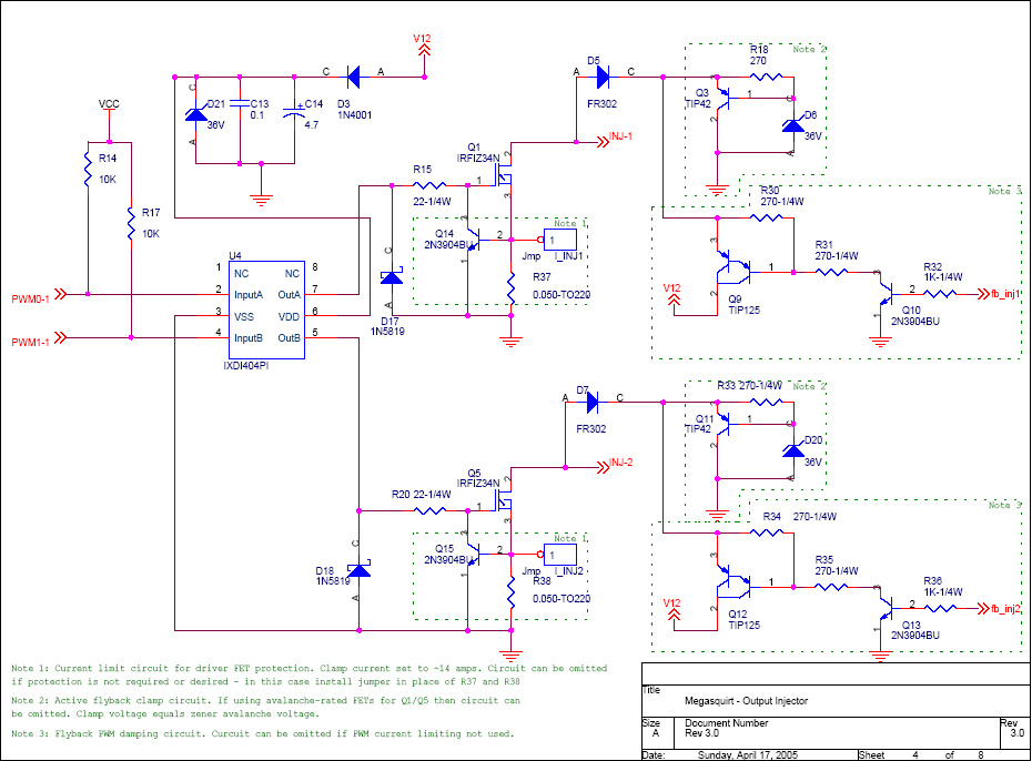
Note 1: Current limit circuit for driver FET protection. Clamp current set to ~14 amps. Circuit can be omitted if protection is not required or desired - in this case install jumper in place of R37 and R38
Note 2: Active flyback clamp circuit. If using avalanche-rated FETs for Q1/Q5 then circuit can be omitted. Clamp voltage equals Zener avalanche voltage.
Note 3: Flyback PWM damping circuit. Circuit can be omitted if PWM current limiting not used.
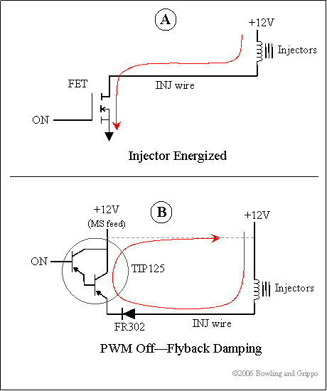
The top drawing A shows the current when the injector driver is on, during the high-time of the PWM waveform. Basically the FET is turned on, energizing the injector. This is the PWM high time, and it depends on the setting of the PWM duty cycle.
The second drawing B is the path when the driver is turned off during PWM flyback damping, or recirculation mode. This occurs during the off time of the PWM current limit. During this time the injector is trying to maintain the current that was there during the PWM on time (see Lenz law). So the injector will generate a current (from the collapsing magnetic field) that flows thru the FR302 diode, the TIP125 transistor, thru the +12V feed and back to the injector. The +12V feed to the MS is used as a path. Note that this is the closed loop path, this is not ground-referenced - the +12V is used as a return path, not as the potential source.
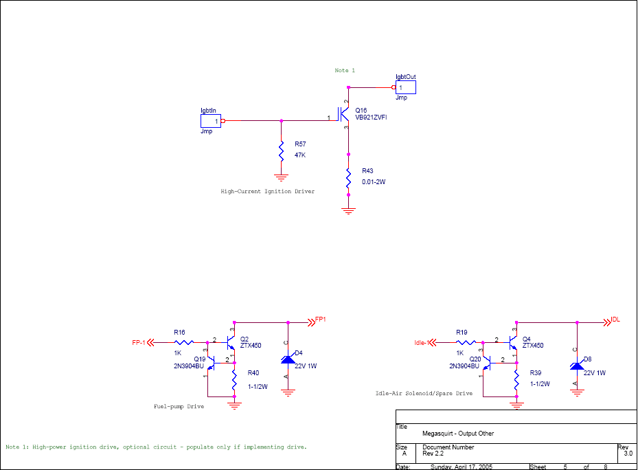
Note 1: High-power ignition drive, optional circuit - populate only if implementing drive.
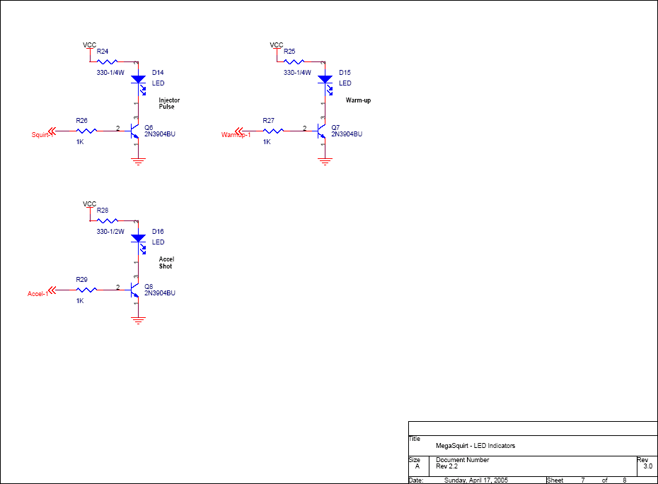
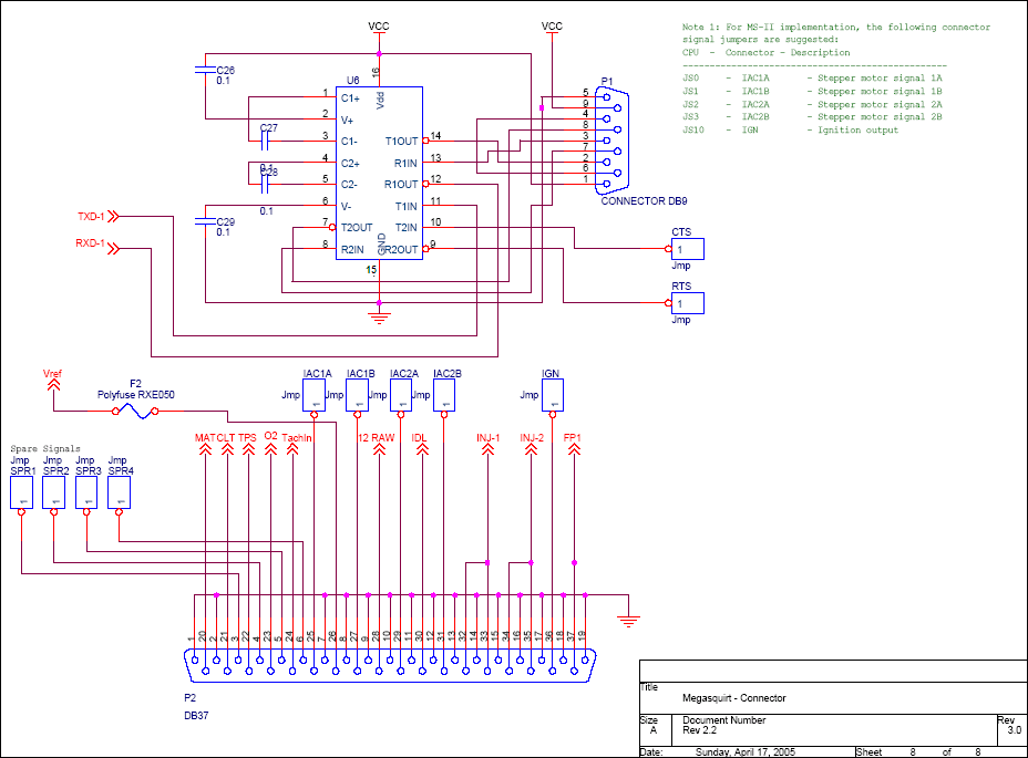
Note 1: For MS-II implementation, the following connector signal jumpers are suggested:
| CPU | Connector | Description |
| JS0 | IAC1A | Stepper motor signal 1A |
| JS1 | IAC1B | Stepper motor signal 1B |
| JS2 | IAC2A | Stepper motor signal 2A |
| JS3 | IAC2B | Stepper motor signal 2B |
| JS10 | IGN or IGBTIN (w/ IGBTOUT->IGN) check manual | Ignition output |
| JS6 | SPR1/CANH | CAN High |
| JS8 | SPR2/CANL | CAN Low |
Variable Reluctor Input Circuit
This is a brief description of a proposed universal input tach trigger circuit for MegaSquirt® V3 main board. This circuit combines several discrete circuits into one input trigger circuit. Additionally, it provides an independently-adjustable trip point/hysteresis setup for use with Variable-Reluctance sensors (VR), Hall sensors, Ford EDIS, and ignition coil primary triggering. The input circuit is protected from overvoltage and can tolerate high voltage up to ±400V. Component selection is not critical and can easily be fulfilled with automotive-temperature devices readily available.
Here is the universal tach input circuit, as tested in PSPICE:
The circuit operation as follows: the tach signal input (from a variable reluctance (VR) sensor, hall sensor, ignition coil primary, or Ford EDIS module) is brought into resistor R100, and is filtered by R100, R101, and C100. R103 provices further current limiting, and C101 is a speedup capacitor arrangement. R102 provides a weak pullup (in case there is no signal or no sensor). D100 clamps voltages higher than 5.7 volts.
PNP transistor Q1 is used as a voltage translation device. It takes advantage of the fact that the voltage drop between the base and emitter is roughly 0.6 volts (depending on the particular transistor, many PNP small-signal transistors can be used), with the emitter always 0.6 volts higher than the base for a PNP. Thus, a zero-crossing bipolar input voltage signal will be "level translated" to 0.6 volts. This translation allows for the use of single-supply operational amplifier use (U3A) to detect zero crossing. It also eliminates the biasing of the op-amp inputs with resistors (which is also an adequate method for tach input triggering) and allows asymmetric hysteresis (more on this below). The emitter-follower setup of the transistor allows for high input impedance and low trigger currents while presenting a low impedance voltage source to the op-amp input, without having to rely solely on the input impedance of the op-amp (and the corresponding op-amp bias and feedback resistors which affect the overall input impedance).
The emitter signal from Q1 is biased by Rbiasq1 to provide emitter-collector current flow. Rseriesq1 feeds the op-amp U3A and is fed into the inverting input.
Transistor Q2 and the associated base resistors Rtriphigh and Rtriplow do a similar function as Q1 in providing the voltage drop between the base-emitter junction. By setting the values of Rtriphigh and Rtriplow the voltage trip point can be set. These two discrete transistors can be replaced by a potentiometer (say 10K). For use with a VR sensor, the transistor base should be at ground potential, or set Rtriplow to 0 ohms (or move potentiometer wiper all the way low). For ignition coil and Hall use, set the trip point voltage to roughly 2.5 volts (make Rtriphigh and Rtriplow equal, say 1K or so, or move the potentiometer wiper to mid point).
The op-amp is really acting as a inverting comparator, with the feedback resistor Rhysteresis providing adjustable hysteresis - this resistor can be replaced with a 100K potentiometer. For a VR sensor the resistance should be high, like 100K, this gives minimum hysteresis. For hall and ignition coil primary use the resistance should be 10K or so (adjust to suit).Note that this is asymmetric hysteresis, it depends on direction of input signal. If the input signal is negative-to-positive transition then the output swings positive-to-negative (opamp inverts) and the trip voltage is very close to the base-emitter voltage drop setpoint of Q2. Now, when the input transitions from positive-to-negative the trip-point setting is modified (by a voltage divider set up by Rseriesq2 and Rhysteresis, with op-amp output low, modifying the op-amp trip voltage seen from Q2). This effect will be shown in the following simulation runs.
It should be noted that the MS interrupt sequence is activated from a high-to-low logic transition (MS-II can trigger on either event, software-configured). Note that the op-amp circuit inverts so that the corresponding input signal is low-to-high transition. For EDIS operation where a high-to-low activation is required, one can either switch the input signals feeding the (+) and (-) terminals of the op-amp, or add another circuit following the op-amp that inverts the digital signal. If using a dual op-amp package then the second op-amp can be set for unity-gain inverting (be sure to bias the op-amp (+) terminal to 2.5 volts or so to set the second op-amp trip point).
Note that if one uses potentiometers for trip point and hysteresis then they should be automotive temp devices of high quality, preferably multi-turn devices. Also, digital potentiometers can be used for these as well, thus allowing potential software control of trip points and hysteresis.
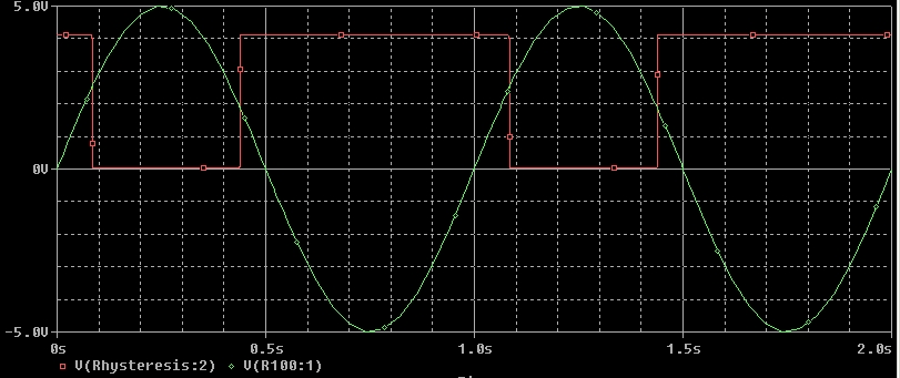
Here are some PSPICE simulation runs of the circuit. Using a +/- 1 volt AC waveform signal input to simulate operation of a VR sensor, the corresponding output transitions are shown:
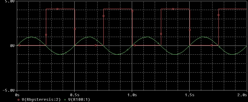
The green signal is the simulated input signal and the red line is the op-amp output. The Q2 bias voltage is set to zero and the hysteresis resistor set to 100K. The important thing to note is the trip points of the red line transition relative to the green line input. Here is a close-up of the negative-to-positive input and the corresponding output (red) signal:
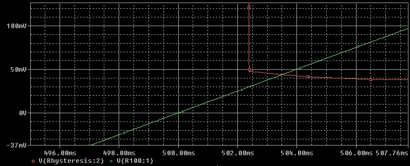
Note that the red line trips at about 30 milliVolts of input signal, which is very close to zero volts relative to the entire span of operating voltage presented in a VR sensor.
Next simulations were run for trip points of 2.5 volts (Rtriphigh = Rtriplow = 4.7K) and with different hysteresis added. This one shows a hysteresis resistor value of 100K:
Note that the green low-to-high transition yields a red line high-to-low transition point of 2.5 volts. On the other side, the transition voltage is at 2 volts, thus a 1/2 volt hysteresis has been added.
Finally, here is a run with the hysteresis resistor lowered to 25K:
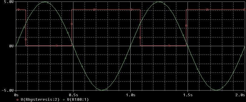
One can see that the green input low-to-high trip point is still 2.5 volts, but the other side trip point is now about 0.5 volts, or a 2 volt hysteresis.
To see how this compares to the current MS tach input circuit waveform response (opto-isolator with Wing diode and Ed and Dave capacitor) here is a frequency response with a 200 Hz waveform (zoomed in):
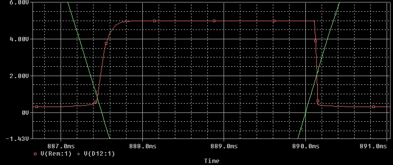
It can be seen that the green low-to-high transition (right-side) is roughly 2 volts and the return transition (left side of image) is 0.8 volts. The positions of the hysteresis trip points are somewhat dependent on RPM due to the filtering effect of the Dave cap. These trip points can be easily reproduced with the new circuit and are basically the same value independent of RPM (excluding input filtering effects).
Finally, a word on component selection. Any general purpose PNP transistor will work for Q1 and Q2, but they need to be the same part number. Paranoid individuals can physically touch the two transistors together such that they are at the same temperature (in order to keep the voltage drops identical due to temperature), but this is not needed in a practical sense. For the op-amp selection, one can use a single-supply op-amp (like the MC34071 or the LM324), or a comparator like a LM393 (with pull-up on output). The main thing to look out for in op-amp choice is the ability for the inputs to swing down to zero volts. Select an op-amp with internal PNP inputs which will allow operation near the lower supply rail. Finally, for primary ignition coil sensing, coil ring may cause multiple triggers that the hysteresis cannot tune out. For this, it is suggested that a 50 - 100 milliHenry inductor (DigiKey DN4548) be added to the input. The inductor will filter out high-frequency oscillations while passing the lower frequency coil transition to the circuit.