Click here for MegaSquirt® MegaManual™ Information, Guides, and Links
Under construction....
The general purpose input/output board (GPIO) board comes partly assembled. All the surface mount devices have already been soldered to the board. These include the processor, and the serial and CAN communication circuits.
There are a number of steps remaining to build your general purpose input/output board. These go under the main stages of:
Each of these steps will be described in considerable detail below.
In this stage, we will assemble and test the power circuits, as well as the peripheral items needed to test the power:
1. Before doing anything else, test the board's power circuit traces and layout. Do this by checking the resistance from the ground to the 5 and 12 Volt supplies. You can do this by checking the resistance between the three holes for the voltage regulator:
| Pins | Resistance |
| 1-2 | |
| 1-3 | |
| 2-3 |
In all cases you should get infinite resistance. If you get less than infinite resistance, and there are no components installed on your board, then there is an error in the manufacture of your board. Please contact the seller for an exchange.
2. Test fit the GPIO board in the case. The GPIO board is designed for the same style case as MegaSquirt® (it won't fit in the same case though, the connector won't allow this). If the PCB is too wide for the case, you can file the heat sink side of the board slightly. A dozen or so seconds with a medium file ought to create enough clearance to allow the board to slide in the case. Then check that the length isn't too long for the case, and file slightly if necessary. Do not remove more than 0.020" (0.5mm) from either the sides or end of the PCB. Be sure to clean the board very well after filing.
3. You will need to make a heat sink out of 0.625" x 0.125" x 5.375" (16mm x 3mm x 136.5mm) aluminum. The heat sink needs to be drilled with a number of holes. Mark these holes by placing the heat sink material against the PCB (be sure to allow room along the edge for the heat sink to slide into the case), and mark the heat sink from the back side with a felt pen. Then drill the heat sink in the center of these marks with a 0.125" (3mm) drill bit. De-burr all the holes, then sand both sides of the heat sink to eliminate any rough spots.
4. Install and solder the 35 pin AMPSEAL connector to the PCB. Be sure to install the connector on the same side of the board as the processor (the side with the silkscreen printed on it). Note that the AMPSEAL connector will interfere with the VB921 circuit closest that end of the board. if you plan to use that circuit, you should trim the mounting lug on the AMPSEAL connector before installing it. This is easiest to do with a fine toothed saw (hack saw blade or similar) - trim it nearly flush with the AMPSEAL connector flange to allow enough room t install and remove the VB921.
5. Install and solder H1 {WM8135-ND}, the 25 x 2 header. Solder all the pins from the bottom side of the PCB. When you have complete assembly of your GPIO board, you will install jumpers {S9000-ND} on all the circuits you plan to use. Note that you don't necessarily have to use the header, you can use wires to jumper the I/O circuits to particular CPU pins, if you prefer.
6. Install and solder the voltage regulator U4 {LM2937-5.0-ND, TO-220 three pin package with mounting hole}. The voltage regulator fits on top of the heat sink at the end nearest D9. Bend the leads on the regulator to allow the three pins to fit in the holes, while still allowing thee mounting hole to line up with the heat sink. Bolt the regulator to the heat sink, then solder the regulator pins in place.
7. Install and solder the C15 capacitor {399-2017-ND, 0.001 µF, 102 marking}. It install in the opposite corner of the PCB from the regulator you just installed.
8. Install and solder the F2 polyfuse {RXEF050-ND}.This installs on the bottom side of the PCB, immediately next to the AMPSEAL connector, near the other components you have just installed. Bent the leads to 90° to make F2 parallel to the PCB - spaced up by about Ľ" (6mm), pointing towards the middle of the board. Be sue it does not contact the bottom the of AMPSEAL connector pins.
9. Install and solder the MOV1 {P7315-ND}. This is the large round black disc. It installs on the bottom side of the board, near C15 which you just installed. Bent the leads to 90° to make the MOV parallel to the PCB - spaced up by about ˝" (12mm), pointing towards the middle of the board. Be sue it does not contact the bottom the of AMPSEAL connector pins.
10. Install and solder the C16 capacitor {399-3584-ND, 22 µF, 226 marking}. This is a polarized capacitor, the side with the + goes towards the nearest edge of the PCB. It is located near the voltage regulator you installed earlier.
11. Install and solder the D10 diode {1N4001DICT-ND}. It is located near the MOV1 you installed earlier (by the AMPSEAL connector). The banded end goes towards the MOV1, away from the nearest edge of the PCB.
12. Install and solder the D12 diode {1N4749ADICT-ND}. It is located beside D10 that you just installed. The banded end goes towards the MOV1, away from the nearest edge of the PCB.
13. Install and solder the D11 diode {1N4001DICT-ND}. It is located beside the voltage regulator, at the end of the heat sink. The banded end goes towards the nearest edge of the PCB, away from C16 you installed earlier.
14. Install and solder the D13 diode {1N4742ADICT-ND}. It is located beside D11 you just installed, at the end of the heat sink. The banded end goes towards the nearest edge of the PCB, away from C16 you installed earlier.
15. If you wish to install a power indicator LED, install R1 {330KQKK-ND, 330 Ohms, orange-orange-brown} and D1 {P301-ND}. These install in the corner of the PCB near the voltage regulator. The LED is installed so that the side with the flat on it (which is the same side as the shorter lead) goes in the square solder pad furthest from R1.
16. Install and solder the F1 polyfuse {RXEF050-ND}. This installs below the middle pin of the voltage regulator.
17. Install and solder the D9 diode {1N4001DICT-ND}. This is located beside the voltage regulator at the end of the heat sink, and beside D11 and D13. The banded end goes closest to the nearest edge of the PCB, like the other adjacent diodes. Solder it from the under side of the PCB, as space is getting tight near the voltage regulator.
18. Install and solder the D19 diode {1N4734ADICT-ND} The banded end goes towards the processor, and away from D9.
19. Install and solder the L1 inductor {M8388-ND}. This is beside F1, which you installed earlier near the voltage regulator.
20. Install and solder the L2 inductor {M8388-ND}. This is located next to L1. Be careful not to allow the exposed leads on L1 and L2 to touch.
21. Install and solder the C17 capacitor {399-3584-ND, 22 µF, 226 marking}. This is a polarized capacitor, the side with the + goes towards the nearest edge of the PCB. It is located near C16 you installed earlier.
22. Install and solder the C18 capacitor {399-4329-ND, 0.1 µF, 104 marking}. This is located next to the F1 polyfuse you installed earlier.
23. Install and solder the C19 capacitor {399-4329-ND, 0.1 µF, 104 marking}. This is located next to the BLD jumper near the edge of the PCB (next to the serial jack).
24. Install and solder the C22 capacitor {399-3559-ND, 4.7 µF, 475 marking}. It is located near the AMPSEAL connector, approximately in the middle. This is a polarized capacitor, the side with the + goes away from the AMPSEAL connector.
25. Install and solder the C23 capacitor {399-4329-ND, 0.1 µF, 104 marking}. This is located beside C22, which you just installed near the AMPSEAL connector.
Unlike MegaSquirt® EFI Controller, the GPIO Board does not use a DB9 connector for serial communications. Instead it uses a 2.5 mm (aka. 3/32") sub-miniature stereo jack, of the same spec used for the Innovate LC-1 wide band controller. This cable is supplied with production GPIO units, but not beta units. If you have a beta GPIO board, or if you have lost your cable, you can build it from Digi-Key parts. To build this cable (if you don't already have one):
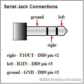
1. Solder the leads from the 2.5mm stereo plug cable {CP-254CS-ND} to the DB9 connector {4109FE-ND}. The wires are soldered to the pins as follows:
| Wire Color | DB9 Pin |
| Red | 3 |
| Black | 2 |
| Green | 5 |
| Yellow | no connection |
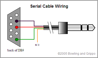
2. Install the hood {976-09RPE-ND} onto the DB9 connector. Be sure to secure the wires in the hood so the the wires will not pull loose from their solder cups.
VR (Variable Reluctor) Circuits
The VR circuits are designed to be configured one way, though clever users can likely find other configurations for other uses. For more info on the VR circuits, see: vr.htm. To assemble the standard circuit (which uses a 'zero-crossing' detector to create a square wave) follow these instructions:
There are 4 VR circuits on the GPIO main board. Each circuit is located within a rectangle on the silkscreen, and these are marked VR1, VR2, VR3, and VR4. You can build any number of these, from zero to all four.
1. Install and solder R1 {10KH-ND, 10K Ohms, ˝W, brown-black-orange}. This is located near the lower left edge of the circuit's silkscreen rectangular layout (when the PCB's copyright notice is at the bottom). Space the resistor off the PCB by approximately 1/4" (3mm).0 6
2. Install and solder R2 {220KEBK-ND, 220K Ohms, red-red-yellow}. All resistors are 1/6 or 1/8 W unless otherwise noted. This is located on the left side of the circuit layout, near the middle (top to bottom). This and all the remaining resistors can be flush against the PCB.
3. Install and solder R3 {2MEBK-ND, 2M Ohms, red-black-green}. This is located immediately above the R2 resistor you just installed.
4. Install and solder R4 {100KEBK-ND, 100K Ohms, brown-black-yellow}. This is located very near the center of the circuit layout.
5. Install and solder R5 {33KEBK-ND, 33K Ohms, orange-orange-orange}. This is located above R3, the resistor you installed earlier on the left side.
6. Install and solder R6 {10KEBK-ND, 10K Ohms, brown-black-orange}. This is located near the op edge of the circuit layout, near the middle (left to right).
7. Install and solder R7 {10KEBK-ND, 10K Ohms, brown-black-orange}. This is located on the right side of the circuit layout.
8. Install and solder R8 {4.7EBK-ND, 4.7K Ohms, yellow-violet-red}. This is located near the top-center of the circuit layout, below R6 you installed earlier.
9. Install and solder R9 {300KEBK-ND, 300K Ohms, orange-black-yellow}. This is located in the upper-right corner of the circuit layout, below R8 that you just installed.
10. Install and solder C1 {478-2454-ND, 0.00047 µF (470pF), 471 marking}. This is located below R2 near the left side of the circuit layout.
11. Install and solder D1 {1N4001DICT-ND}. This is located between R4 and C2, near the lower-middle of the circuit layout. The banded end is positioned away from R1 (and the CPU), as shown on the silkscreen.
12. Install and solder Q1 {2N3904FS-ND}. This is located near the center of the circuit layout. The transistor has a flat side and a curved side. The flat side faces the bottom of the PCB, the side with the copyright notice. On this and the other transistor, you have to spread the leads slightly to match the holes in the PCB. This expanded footprint spacing does make the soldering much easier.
13. Install and solder Q2 {2N3904FS-ND}. This is located near the right-middle of the circuit layout. The transistor has a flat side and a curved side. The flat side faces the bottom of the PCB, the side with the copyright notice.
14. Install and solder Q3 {2N3904FS-ND}. This is located near the bottom-right of the circuit layout. The transistor has a flat side and a curved side. The flat side faces the bottom of the PCB, the side with the copyright notice.
15. Install and solder C2 {478-2448-ND, 47 pF, 470 marking}. This is located in the bottom center of the circuit layout.
GPO (General Purpose Output) Circuits
The GPOx circuits are designed to be configured in one of three ways, though clever users can likely find other configurations for other uses. For more info on the GPOx circuit, see: gpo.htm. To assemble the standard circuit follow these instructions:
1. Install and solder R1 {1.0KEBK-ND}, the 1K Ohm base resistor for the transistor. It is located near the edge of the circuit, furthest from the heat sink.
2. Install and solder R2 {330EBK-ND}, the 330 Ohm current limiting resistor. It is located near the center of the circuit.
3.
4. Install and solder Q1 {PN2222AD26ZCT-ND}. The transistor has a flat side and a curved side. The flat side faces the top of the PCB, the side with the heat sink.
General Purpose Input Circuits
Note that on the beta boards only, the resistor R2 is not connected to the Ampseal connector. It is connected to ground at the other end. R2 is used mostly in applications that need to respond rapidly to voltage changes, such as an EGO signal. If you install R2, you should jumper it to the closest end of R1.
1.
2.
3.
4.
Pulse Width Modulation Output Circuits
1. Install and solder R1 {1.0KEBK-ND, 1K Ohm, brown-black-red} near the left side of the circuit.
2. Install and solder R2 {1.0H-ND, 1 Ohm} near the left side of the circuit. This resistor is used if you wish to measure the current through the circuit using and oscilloscope. These can be jumpered with a snipped of lead if the device the circuit controls limits current (most do unless they are connected directly to a voltage source). If you require the input circuit to limit current, you should change R2 from it's 1 Ohm value to a higher value that will limit the current (for example, for a 0.5 Amp limit on a 12 Volt source, you would use a 12/0.5 = 24+ Ohm resistor).
3. Install Q1, the TIP120 NPN transistor {497-2539-5-ND}. These are located on the heat-sink, near the voltage regulator you installed earlier. Bend the leads so that the mounting hole in the tab lines up with the hole in the heat sink, and solder it in place.
4.Install and solder D1 {1N4749ADICT-ND}, the 22V flyback Zener diode. Be sure the end nearest the band is closest to the heat sink. Inspect the installed diode to be sure the lead does not touch the heat sink (bend the lead or file the heat sink in there is contact).
VB921 Ignition Output Circuits
1. Install Q1 {497-2716-5-ND}, the VB921 ignition coil driver [or TIP120, 497-2539-5-ND, if you are using the circuit as a general output and not an ignition coil driver]. These are located on the heat-sink, near the voltage regulator you installed earlier. Bend the leads so that the mounting hole in the tab lines up with the hole in the heat sink, and solder it in place.
2. Install and solder R1 {1.0KEBK-ND, 1K Ohm, brown-black-red}. These are located between the VB921 on the heat sink and the GPOx circuits, and are labeled as to which VB921 each resistor corresponds to.
3. If you are not using a VBx circuits as ignition coil drivers, but instead are using it as a general purpose output with the TIP120 (to control relay, solenoids, etc.) then install D1 {1N4749ADICT-ND}, the flyback 22V Zener diode.
EGT (Exhaust Gas Temperature) Circuits
The EGT circuits are designed to be configured one of two ways: exhaust gas temperature measurement with a an AD595 IC, or a regular NTC (negative temperature coefficient) temperature measurement circuit (with standard automotive coolant or air temperature sensors), though clever users can likely find other configurations for other uses. For more info on the EGT circuits, see: egt.htm. To assemble the standard circuit follow these instructions:
1. Install and solder the AD595, the EGT IC. Be careful to get the notched end furthest from the ampseal connector. Ensure that the IC is fully seated before soldering. Do not use a socket for this IC (the chip must be in thermal contact with the PCB to work accurately).
2. Install and solder R2 {10.0KXBK-ND, 10.0K Ohms}.
3. Install and solder R4 {15.0KXBK-ND, 15.0K Ohms}.
4.Install and solder C1 {399-4146-ND, 1000 pF}.
5. Install and solder C2 {399-4289-ND, 0.22 µF}
6. Install and solder R1 {1.0KEBK-ND, 1.0K Ohms}.
7. In general, do not install R5, which is for non-grounded thermocouples only.
8. Using silver solder, solder the thermocouple wires to the pads nearest the notched end of the AD595 IC. The alumel connection is labeled "a", the chromel connection is labeled "c". You can run thermocouple wire to a specialized thermocouple jack mounted on the case end. See: www.process-controls.com/ASB_Heat/thermocouples_plugs.htm, for example.
1. Install and solder R1 {1.0KEBK-ND, 1.0K Ohms}.
2. Install and solder R3 {2.49KXBK-ND, 2.49K Ohms}.
3.Install and solder C1 {P4962-ND, 1.0 µF}.
4. Install and solder C2 {399-4202-ND, 0.001 µF}
5. Install a jumper (make it from a snipped off lead) between the adjacent vias marked "a" and "x".
There are 25 I/O ports available on the processor, and the GPIO board has 25 of these circuits. You can use all of these, or as few as you want.
Circuit | CPU Port | AMP pin number |
| 12 Volts (IN) | n/a | 1 |
| VR1 | PT0 | 2 |
| GPI4 | PAD07 | 3 |
| GPI5 | PAD06 | 4 |
| GPI1 | PAD00 | 5 |
| GPI2 | PAD01 | 6 |
| GPO2 | PM3 | 7 |
| GPO3 | PM5 | 8 |
| GPO4 | PB4 | 9 |
| GPO1 | PM4 | 10 |
| VB1 | PE0 (PE0 is input only, so another port must be jumpered to VB1 to use that circuit) | 11 |
| VB2 | PA0 | 12 |
| CANH | (MCP2551) | 13 |
| VR3 | PT5 | 14 |
| VR2 | PT6 | 15 |
| CANL | (MCP2551) | 16 |
| Ground | n/a | 17 |
| Ground | n/a | 18 |
| Ground | n/a | 19 |
| Ground | n/a | 20 |
| Spare Pin (Serial Tx) | 12V/GND/5V - or serial | 21 |
| Spare Pin (Serial Rx) | 12V/GND/5V - or serial | 22 |
| VB3 | PE4 | 23 |
| EGT1 | PAD05 | 24 |
| EGT3 | PAD03 | 25 |
| EGT4 | PE1 | 26 |
| EGT2 | PAD04 | 27 |
| 5 Vref (OUT) | 28 | |
| VR4 | PT7 | 29 |
| GPI3 | PAD02 | 30 |
| PWM1 | PT4 | 31 |
| PWM2 | PT3 | 32 |
| PWM3 | PT2 | 33 |
| PWM4 | PT1 | 34 |
| VB4 | PM2 | 35 |
Note that you can test the input and output of each circuit independently of the processor. In addition to the ampseal connector and 2x25 header, you can also probe the circuits at the circuit itself. In general, the ampseal side of the circuit is labeled with a via marked "a", and the processor side is labeled with a via marked "p" (except for VR4, where these are backwards on the beta boards - so be aware).